



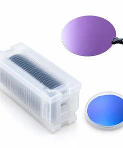

IR1 High-Resistivity FZ Intrinsic Silicon Wafers, 1-8 Inch
Price range: $2.00 through $590.00
High-Resistivity FZ Intrinsic Silicon Wafers – 1–8 Inch
Product Description
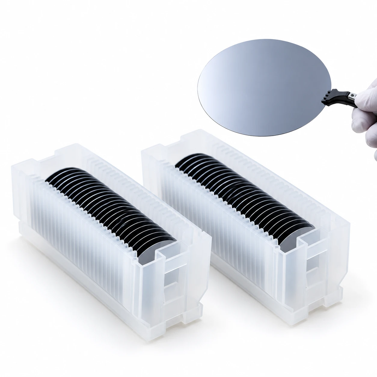
High-resistivity Float Zone (FZ) intrinsic silicon wafers are designed
for semiconductor research, spectroscopy, thin-film deposition,
microscopy and advanced materials applications where high-purity
silicon substrates are required.
Float Zone silicon provides high-purity single-crystal material and is
available in multiple wafer diameters, thicknesses and crystal
orientations. High-resistivity grades are available for applications
requiring reduced free-carrier concentration and improved electrical
isolation.
Wafer diameters from 1 inch to 8 inches are available. Standard
substrate thicknesses include 525 μm, 625 μm and 725 μm, while
customized thicknesses from approximately 50 μm to 12 mm can also
be supplied.
Technical Parameters
| Material | Single-Crystal Silicon |
| Crystal Growth Method | Float Zone (FZ) |
| Conductivity Type | Intrinsic / High-Resistivity Silicon |
| Wafer Diameter | 1–8 Inch |
| Surface Finish | Single-Side Polished |
| Standard Thickness | 525 μm / 625 μm / 725 μm |
| Custom Thickness | 50 μm – 12 mm |
| Crystal Orientation | (100) / (110) / (111) |
| Resistivity | High-Resistivity Grades Available, up to approximately 100,000 Ω·cm |
Geometry & Surface Quality
| TIR | < 3 μm |
| TTV | < 10 μm |
| BOW | < 10 μm |
| Surface Roughness | < 0.5 nm |
| Particle Count | < 10 particles for size > 0.3 μm |
Product Features
- High-purity Float Zone single-crystal silicon
- High-resistivity intrinsic silicon options
- Wafer diameters from 1 inch to 8 inches
- Single-side polished surface
- (100), (110) and (111) crystal orientations available
- Low surface roughness for surface analysis applications
- Standard and custom substrate thicknesses available
- Suitable for advanced semiconductor and materials research
Applications
- PVD thin-film deposition substrates
- CVD thin-film deposition substrates
- Magnetron sputtering
- X-ray diffraction (XRD)
- Infrared spectroscopy
- Fluorescence spectroscopy
- SEM scanning electron microscopy
- AFM atomic force microscopy
- Ultra-flat laboratory substrates
- Molecular beam epitaxy (MBE) research
- X-ray analysis
- Semiconductor and crystal materials research
Customization
Multiple stock specifications are available. Wafer diameter,
substrate thickness, crystal orientation and resistivity can be
selected according to customer requirements.
For quotation, please provide the required wafer diameter, thickness,
crystal orientation and resistivity range.
| Size | 1-Inch Intrinsic Silicon Wafer / DSP / Undoped / Resistivity Above 1K Ohm-cm, 1-Inch Intrinsic Silicon Wafer / SSP / Undoped / Resistivity Above 1K Ohm-cm, 10X10 MM High-Resistivity Silicon Square, 15X15 MM High-Resistivity Silicon Square, 2-Inch Intrinsic Silicon Wafer / DSP / Undoped / Resistivity Above 10K Ohm-cm, 2-Inch Intrinsic Silicon Wafer / DSP / Undoped / Resistivity Above 1K Ohm-cm, 2-Inch Intrinsic Silicon Wafer / SSP / Undoped / Resistivity Above 10K Ohm-cm, 2-Inch Intrinsic Silicon Wafer / SSP / Undoped / Resistivity Above 1K Ohm-cm, 20X20 MM High-Resistivity Silicon Square, 3-Inch Intrinsic Silicon Wafer / DSP / Undoped / Resistivity Above 10K Ohm-cm, 3-Inch Intrinsic Silicon Wafer / DSP / Undoped / Resistivity Above 1K Ohm-cm, 3-Inch Intrinsic Silicon Wafer / SSP / Undoped / Resistivity Above 10K Ohm-cm, 3-Inch Intrinsic Silicon Wafer / SSP / Undoped / Resistivity Above 1K Ohm-cm, 3-Inch Intrinsic Silicon Wafer / SSP / Undoped / Resistivity Above 20K Ohm-cm, 4-Inch FZ Intrinsic Silicon Wafer / DSP / Resistivity Above 100K Ohm-cm, 4-Inch FZ Intrinsic Silicon Wafer / SSP / Resistivity Above 100K Ohm-cm, 4-Inch Intrinsic Silicon Wafer / DSP / Undoped / Resistivity Above 10K Ohm-cm, 4-Inch Intrinsic Silicon Wafer / DSP / Undoped / Resistivity Above 1K Ohm-cm, 4-Inch Intrinsic Silicon Wafer / SSP / Orientation 100 / 250 UM / Resistivity Above 8K Ohm-cm, 4-Inch Intrinsic Silicon Wafer / SSP / Undoped / Resistivity Above 10K Ohm-cm, 4-Inch Intrinsic Silicon Wafer / SSP / Undoped / Resistivity Above 1K Ohm-cm, 4-Inch Intrinsic Silicon Wafer / SSP / Undoped / Resistivity Above 20K Ohm-cm, 5X5 MM High-Resistivity Silicon Square, 6-Inch Intrinsic Silicon Wafer / DSP / Undoped / Resistivity Above 10K Ohm-cm, 6-Inch Intrinsic Silicon Wafer / DSP / Undoped / Resistivity Above 1K Ohm-cm, 6-Inch Intrinsic Silicon Wafer / SSP / Orientation 100 / 380 UM / Resistivity Above 8K Ohm-cm, 6-Inch Intrinsic Silicon Wafer / SSP / Undoped / Resistivity Above 10K Ohm-cm, 6-Inch Intrinsic Silicon Wafer / SSP / Undoped / Resistivity Above 1K Ohm-cm, 8-Inch Intrinsic Silicon Wafer / DSP / Orientation 100 / 675 UM / Resistivity Above 20K Ohm-cm, 8-Inch Intrinsic Silicon Wafer / SSP / Orientation 100 / 700 UM / Resistivity Above 20K Ohm-cm, 8-Inch Prime Intrinsic Silicon Wafer / DSP / Orientation 100 / Resistivity Above 1K Ohm-cm, 8-Inch Prime Intrinsic Silicon Wafer / SSP / Orientation 100 / Resistivity Above 1K Ohm-cm, 8X8 MM High-Resistivity Silicon Square |
|---|
Be the first to review “IR1 High-Resistivity FZ Intrinsic Silicon Wafers, 1-8 Inch”
Related products

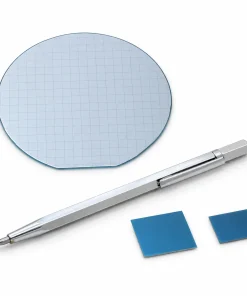
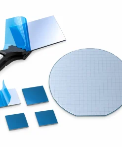
Silicon Wafers
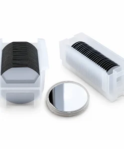
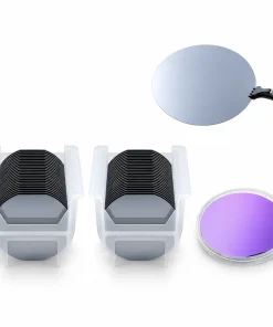
Silicon Wafers


Silicon Wafers

Silicon Wafers
Reviews
There are no reviews yet.