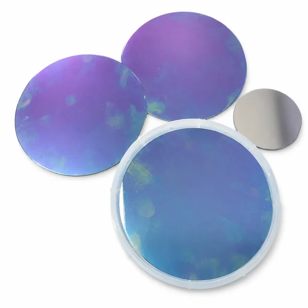
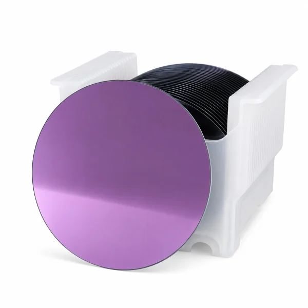
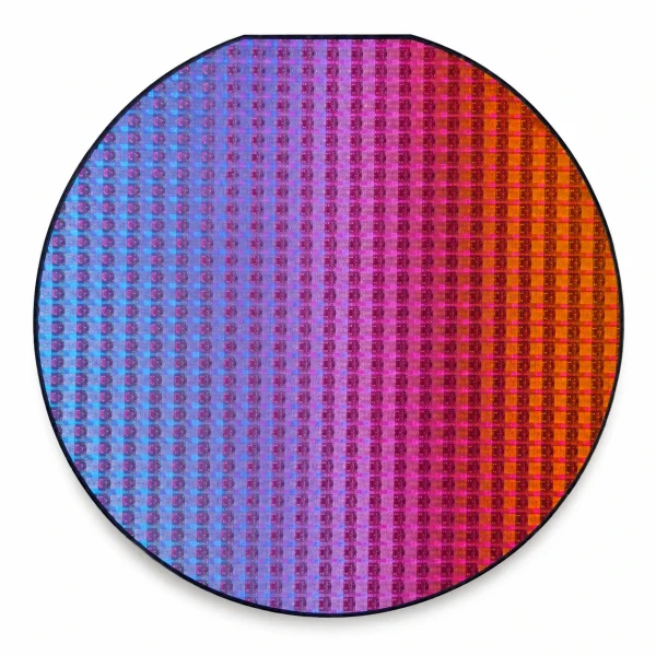
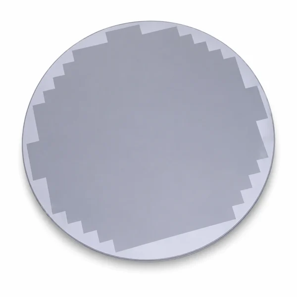
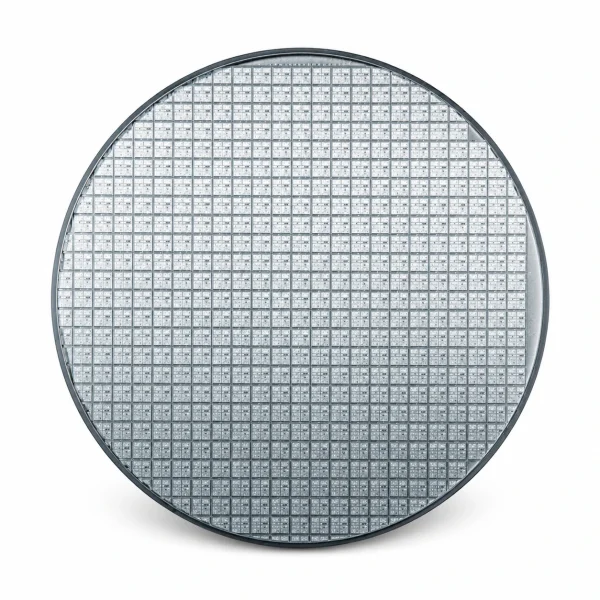
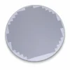
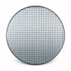
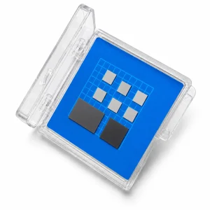
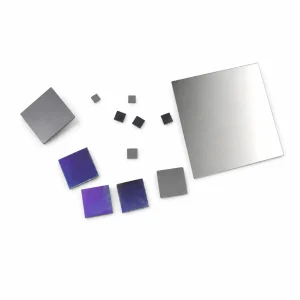
1-Inch High-Purity SSP Silicon Wafer with Thermal SiO₂
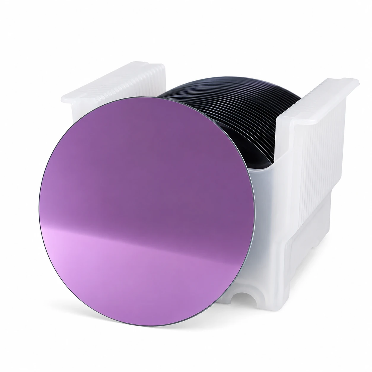
Thermal Oxidation
Thermal oxidation forms a silicon dioxide layer on the silicon surface.
The process is performed at elevated temperatures in the presence of
an oxidizing agent and is known as thermal oxidation.
Thermal oxide layers are typically grown in horizontal tube furnaces
at temperatures ranging from 900°C to 1200°C using wet or dry oxidation.
Compared with oxide layers deposited by CVD, thermally grown oxide
layers provide higher uniformity and higher dielectric strength.
They are suitable as insulating dielectric layers and are widely used
in silicon-based devices as doping barriers and surface dielectric layers.
Applications
- Etch rate measurement
- Metal wire bonding testing
- Metal wafer bonding
- Electrical insulation layer
Available Wafer Sizes
| Wafer Type | 1 Inch | 2 Inch | 3 Inch | 4 Inch | 5 Inch | 6 Inch | 8 Inch | 12 Inch |
|---|---|---|---|---|---|---|---|---|
| Single-Side Polished Silicon Wafer | 1 Inch | 2 Inch | 3 Inch | 4 Inch | 5 Inch | 6 Inch | 8 Inch | 12 Inch |
| Double-Side Polished Silicon Wafer | — | 2 Inch | 3 Inch | 4 Inch | 5 Inch | 6 Inch | — | — |
| Lapped Silicon Wafer | — | 2 Inch | 3 Inch | 4 Inch | 5 Inch | 6 Inch | — | — |
| Intrinsic FZ High-Resistivity Silicon Wafer | — | 2 Inch | 3 Inch | 4 Inch | 5 Inch | 6 Inch | — | — |

Reviews
There are no reviews yet.