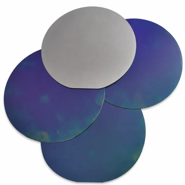
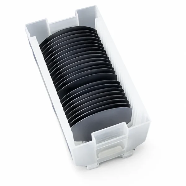
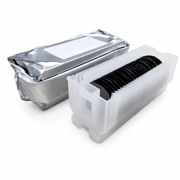
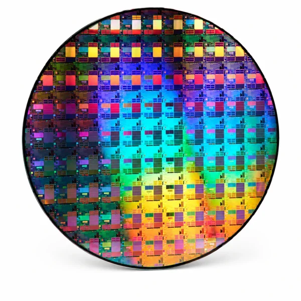
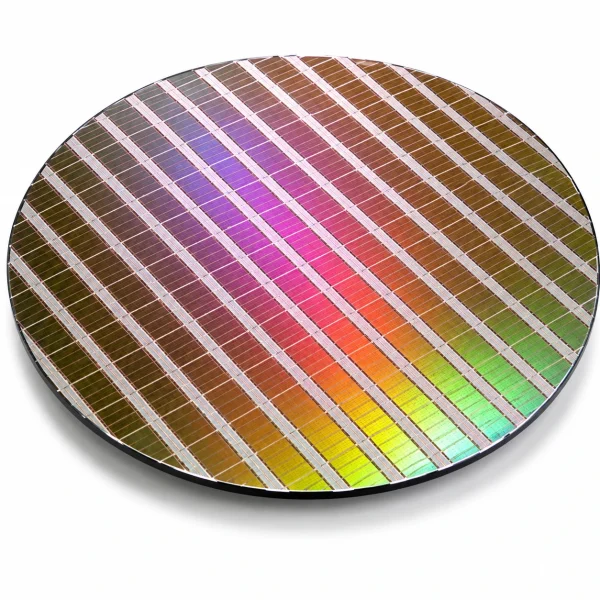
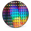
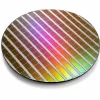
Single-Side Polished Silicon Wafer
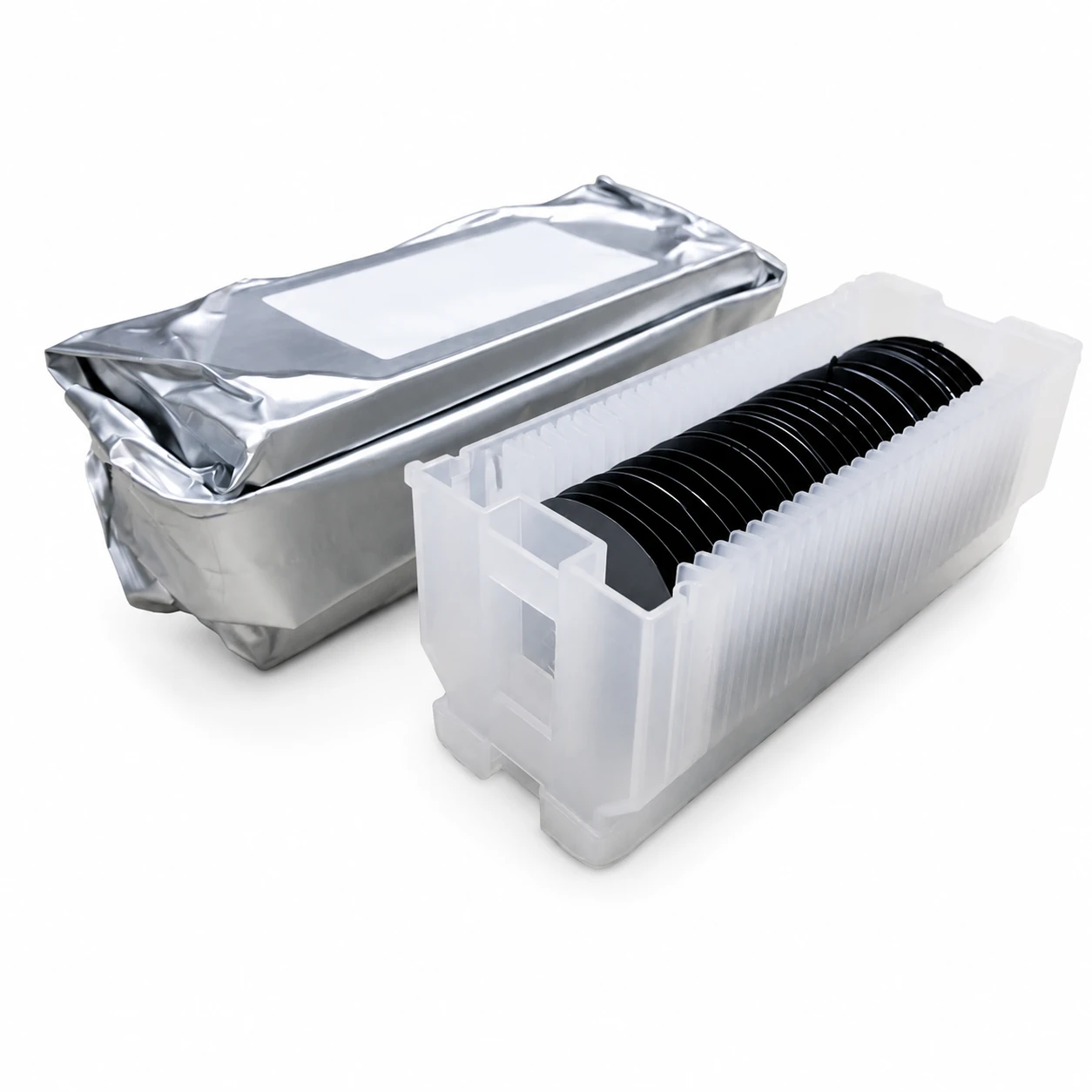
Product Specifications
| Product | Single-Side Polished Silicon Wafer |
| Growth Method | Czochralski (CZ) Single Crystal |
| Diameter & Tolerance | 25.4 ± 0.4 mm |
| Doping Type | N-Type: Phosphorus (P), Arsenic (As), Antimony (Sb) P-Type: Boron (B) |
| Crystal Orientation | <111> / <100> |
| Resistivity | 0.001–50 Ω·cm |
| Custom Resistivity | Available according to customer requirements |
Process Parameters
| TIR | <3 μm |
| TTV | <10 μm |
| BOW | <10 μm |
| Surface Roughness | <0.5 nm |
| Particle Count | <10 for particle size >0.3 μm |
Applications
- Synchrotron radiation sample substrates
- PVD / CVD coating substrates
- Magnetron sputtering sample growth
- XRD analysis
- SEM analysis
- Atomic force microscopy analysis
- Infrared spectroscopy analysis substrates
- Fluorescence spectroscopy analysis substrates
- Molecular beam epitaxy growth substrates
- X-ray analysis of crystalline semiconductor materials
- Microfluidic silicon substrates
- Nanoimprint silicon substrates
- Two-dimensional material substrates



Reviews
There are no reviews yet.