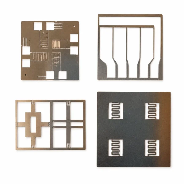




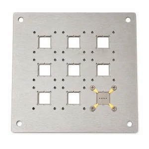
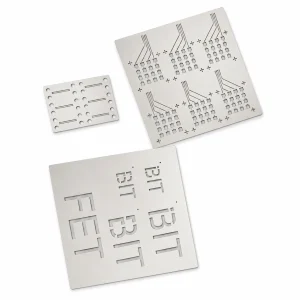
Stainless Steel Shadow Mask for Interdigitated Electrodes & Photodetectors
Manufacturing Methods
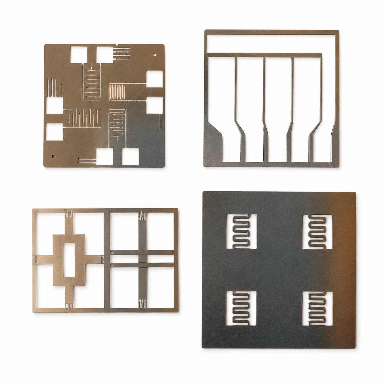
Stainless steel shadow masks are mainly manufactured using
high-precision chemical etching or laser cutting and welding processes.
Process Specifications
| Process | Material / Thickness | Feature Size | Error | Notes |
|---|---|---|---|---|
| Chemical Etching | 304 Stainless Steel / 0.3 mm | 0.4 mm (400 µm) line width 0.4 mm (400 µm) opening |
30–60 µm | Fast processing and relatively low cost |
| High-Precision Chemical Etching | Stainless Steel | 0.1 mm (100 µm) line width | Solid area: 30 µm Opening area: 60 µm |
Suitable for interdigitated electrode shadow masks. Pattern design should take the process error into account. |
| Ultra-High-Precision Laser Processing | Stainless Steel | 0.04 mm (40 µm) line width | 20 µm | Higher precision and higher cost |
Applications
Shadow masks can be used in electron-beam evaporation,
thermal evaporation and magnetron sputtering equipment
to fabricate patterned thin films and electrodes for:
- OPV devices
- OLED devices
- Perovskite solar cells
- Photodetectors
- Field-effect transistors
Process Notes
Chemically etched shadow masks generally have a smoother surface
and better flatness, but the price is relatively higher.
High-precision laser-cut and welded masks may have a slightly rougher
surface. They are generally polished and can meet normal laboratory
requirements. Customers with special requirements should specify
them in advance.
Drawing Requirements
Please provide a CAD drawing whenever possible.
If a CAD drawing cannot be provided, please provide a sketch
that accurately describes the required shadow mask specifications.

Reviews
There are no reviews yet.