


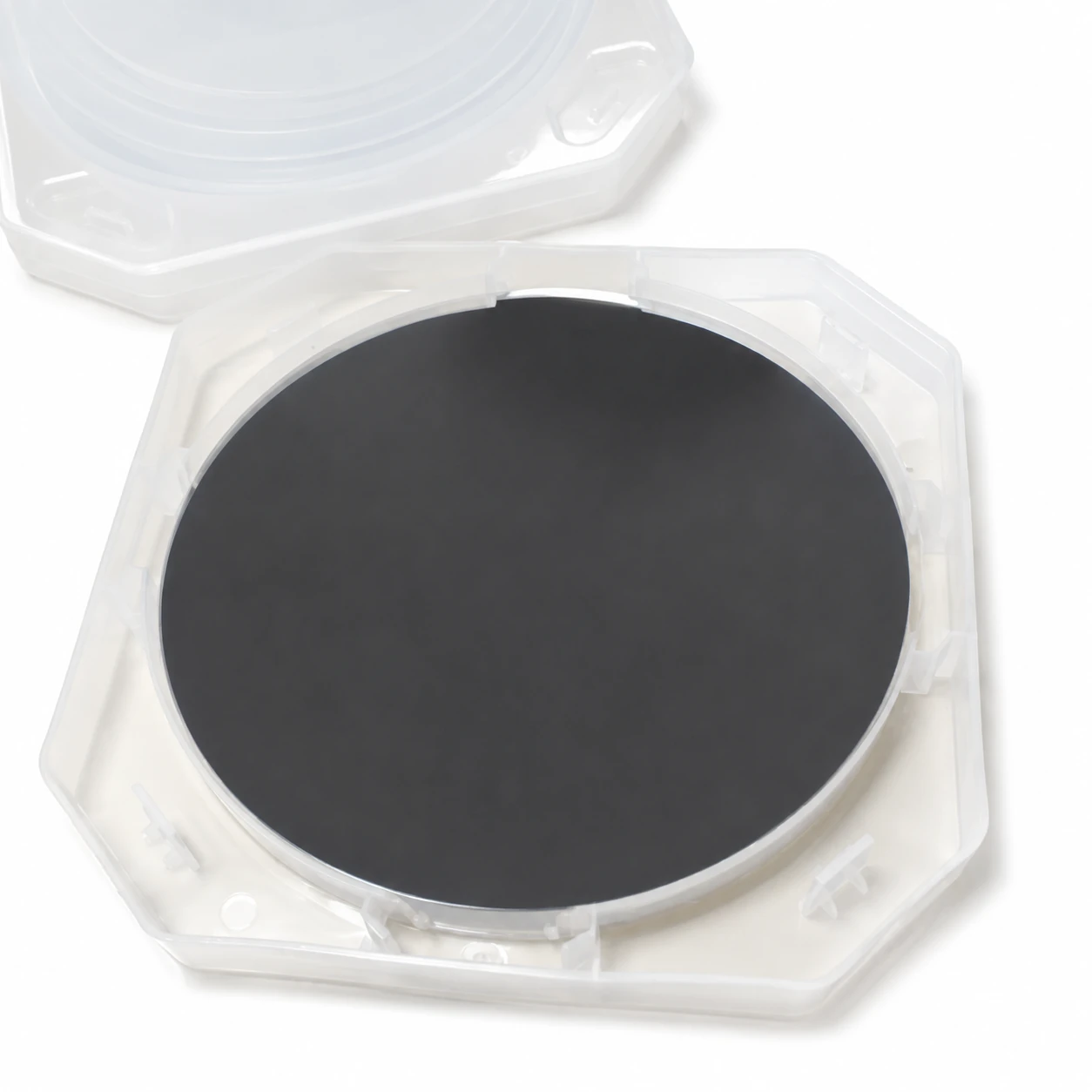
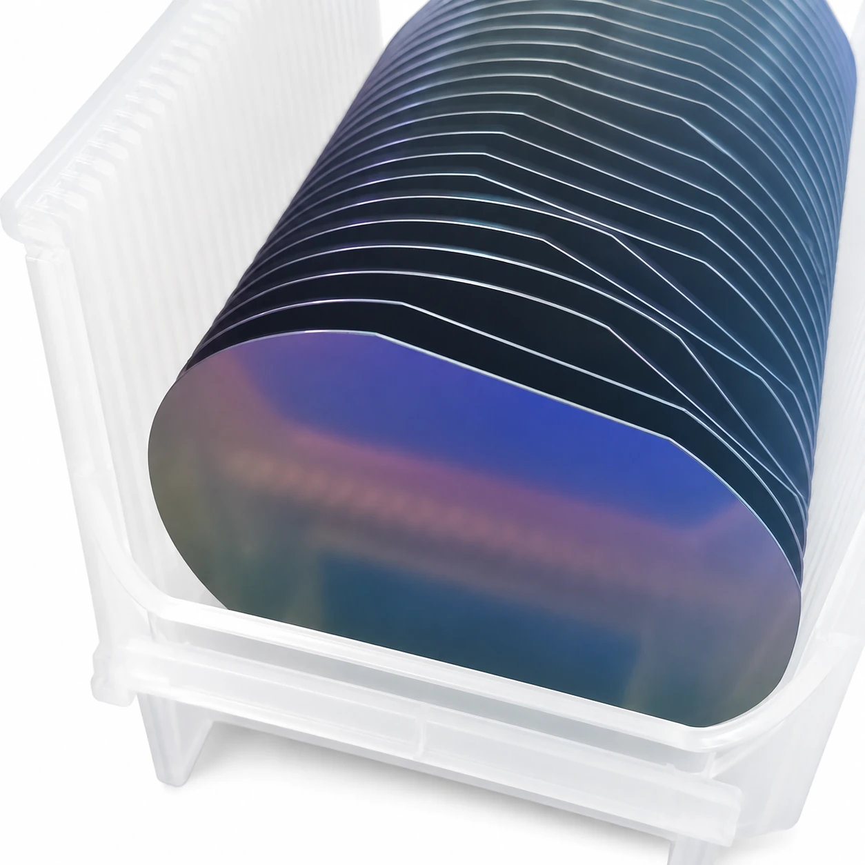
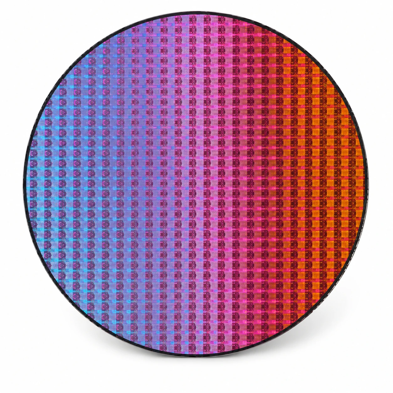
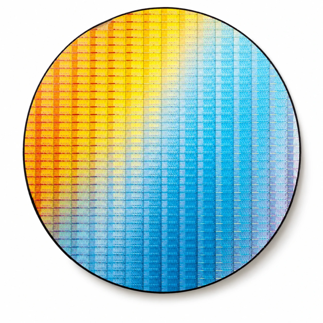
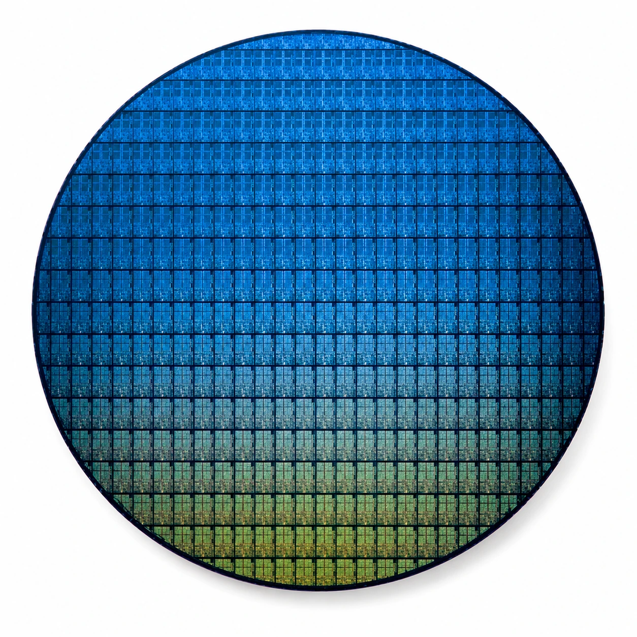
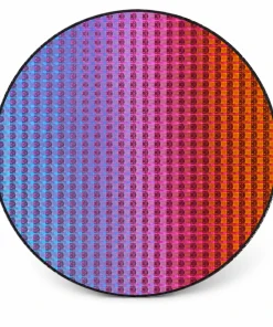
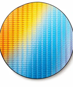
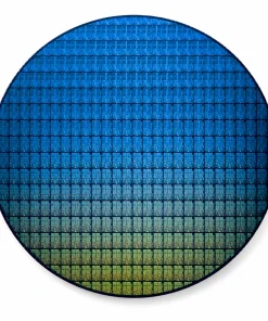
IS1 6-Inch SSP Silicon Wafer Substrate for IGZO TFT & Nanoimprint
Price range: $33.00 through $56.00
6-Inch Single-Side Polished Silicon Wafer
Product Specifications
| Product Name | 6-Inch Single-Side Polished Silicon Wafer |
| Growth Method | Czochralski Single Crystal (CZ) |
| Diameter & Tolerance | 150 ± 0.4 mm |
| Doping Type | N-Type (Phosphorus, Arsenic, Antimony); P-Type (Boron) |
| Crystal Orientation | <100>, <111> |
| Resistivity | 0.001–50 Ω·cm, customizable according to customer requirements |
| TIR | < 3 µm |
| TTV | < 10 µm |
| BOW | < 10 µm |
| Surface Roughness | < 0.5 nm |
| Particle Count | < 10 for particle size > 0.3 µm |
Available Wafer Sizes
| Wafer Type | 1 Inch | 2 Inch | 3 Inch | 4 Inch | 5 Inch | 6 Inch | 8 Inch | 12 Inch |
|---|---|---|---|---|---|---|---|---|
| Single-Side Polished Silicon Wafer | 1 Inch | 2 Inch | 3 Inch | 4 Inch | 5 Inch | 6 Inch | 8 Inch | 12 Inch |
| Double-Side Polished Silicon Wafer | — | 2 Inch | 3 Inch | 4 Inch | 5 Inch | 6 Inch | — | — |
| Lapped Silicon Wafer | — | 2 Inch | 3 Inch | 4 Inch | 5 Inch | 6 Inch | — | — |
| Intrinsic High-Resistivity Silicon Wafer | — | 2 Inch | 3 Inch | 4 Inch | 5 Inch | 6 Inch | — | — |
Typical Applications
- Synchrotron radiation sample carriers
- PVD/CVD thin-film deposition substrates
- Magnetron sputtering growth samples
- XRD analysis
- SEM analysis
- Atomic force microscopy analysis
- Infrared spectroscopy analysis
- Fluorescence spectroscopy analysis
- Molecular beam epitaxy growth substrates
- X-ray analysis of crystalline semiconductors
- TFT thin-film transistor substrates
- Nanoimprint substrates
- Two-dimensional material substrates
| Size | 6-Inch SSP Silicon Wafer / Extra Thick / 1000 UM, 6-Inch SSP Silicon Wafer / Standard / Recommended, Custom Specifications Available |
|---|
Be the first to review “IS1 6-Inch SSP Silicon Wafer Substrate for IGZO TFT & Nanoimprint”
Related products

Substrates & Conductive Materials
Price range: $108.00 through $146.00
Substrates & Conductive Materials
Price range: $4.00 through $38.00
Substrates & Conductive Materials
Price range: $40.00 through $183.00

Substrates & Conductive Materials
HW1 High-Purity Single-Crystal Silicon Wafers, SSP/DSP, 1-12 Inch
Price range: $12.00 through $108.00
Substrates & Conductive Materials
Price range: $25.00 through $146.00

Substrates & Conductive Materials
Price range: $42.00 through $167.00
Substrates & Conductive Materials
Price range: $4.00 through $108.00
Substrates & Conductive Materials
HC1 High-Purity Single-Crystal Silicon Wafer Substrates for SEM & Optical Research
Price range: $2.00 through $42.00
Reviews
There are no reviews yet.